|
|
The Programmable CVD Reactor Project |
Chemical vapor deposition (CVD) is a widely used unit operation for thin film device production in the semiconductor manufacturing industry. The continuing reduction of device feature size, growing scale of device integration, and increasing substrate (wafer) size motivate development of the new CVD equipment and processes necessary to sustain the advancement of microelectronic technology. Current CVD reactor designs do not provide for direct control of gas composition across the wafer surface to counteract reactant depletion and other non-uniformity generators. Furthermore, current designs cannot intentionally generate, control, and measure gas phase composition gradients across the wafer surface. In short, current processes lack the flexibility to program across-wafer spatial distributions of chemical composition or other film qualities, either for uniformity or for intentional non-uniformity.
The exploratory research program described here focuses on the design of a CVD reactor that will enable across-wafer spatial control of deposition characteristics. An existing CVD reactor at the University of Maryland is currently being modified (see figures below) to generate data for developing a detailed simulator for reactor design and operation. The prototype gas showerhead assembly to be tested in the research program currently is under construction; computer simulation methods are also being developed to evaluate the actuation capabilities of this programmable reactor and establish its process simulation, optimization, sensing, and control requirements. In addition to the immediate semiconductor manufacturing benefits of this reactor configuration, its design will establish a prototype for the next generation of chemical vapor deposition reactors for use in a materials development environment for conducting combinatorial CVD studies to rapidly evaluate new processes and materials.
|
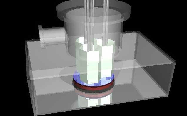
Design of the three-segment programmable reactor system prototype.
>> Larger view |
In alphabetical order:
This project currently is supported by the National Science Foundation and the National Institute of Standards and Technology.
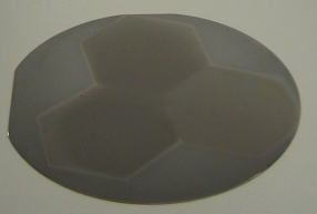
Link to images of the initial wafers produced by the 3-zone prototype
|
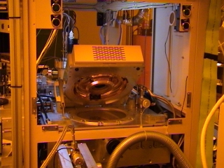
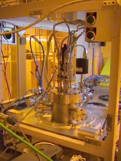
The Ulvac CVD cluster tool reactor chamber prior to modification.
>> Larger view |

|
View of the three-zone prototype showerhead -- 4/4/02
>> Larger view |
|
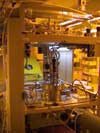
A view of the three-segment prototype which includes the feed gas valve assembly.
>> Larger view |
|
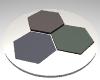
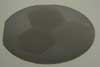
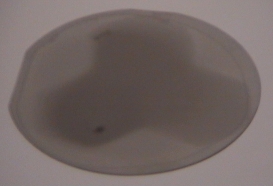
Wafer produced by the programmable reactor during the week of 4/02. Showerhead/wafer spacing = 1.5 mm
resulting in a sharp pattern.
>> Larger view |
|
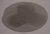
Wafer produced by the programmable reactor during the week of 4/02. Showerhead/wafer spacing = 3.5 mm
resulting in a more inter-segment diffusion.
>> Larger view |

|
Maintained by
R. A. Adomaitis |