News Story
Abshire is part of new DARPA/SRC JUMP 2.0 Center

Professor Pamela Abshire (ECE/ISR) is a co-PI in the new DARPA/SRC JUMP 2.0 Center, “CogniSense: The Center on Cognitive Multispectral Sensors.” Professor Saibal Mukhopadhyay of the Georgia Institute of Technology is the principal investigator. CogniSense is one of seven JUMP 2.0 centers being announced this fall. It is funded for five years.
The new center brings together 20 researchers from 13 universities:
Mingoo Seok, Xiaofan Fred Jiang, Columbia University
Alyosha Christopher Molnar, Cornell University
Saibal Mukhopadhyay (PI), Justin Romberg, Muhannad Bakir, Georgia Institute of Technology
Cheng Huang, Iowa State University
Jelena Notaros, Massachusetts Institute of Technology
Vijay Raghunathan, Stanley Chan, Purdue University
Tingyi Gu, University of Delaware
Q. Jane Gu, University of California, Davis
James Buckwalter, Jonathan Klamkin, University of California, Santa Barbara
Amit Trivedi, Inna Partin Vaisband, University of Illinois, Chicago
Pamela Abshire, University of Maryland
Michael Flynn, David Blaauw, Hun Seok Kim, University of Michigan
About the DARPA JUMP program
The Defense Advanced Research Projects Agency (DARPA) is collaborating with the Semiconductor Research Corp. (SRC) and a consortium of defense and semiconductor companies to launch the second iteration of the Joint University Microelectronics Program (JUMP 2.0). JUMP 2.0 builds off an earlier iteration of the SRC-led collaboration that was formed in 2018 to support university research centers focused on keeping the U.S. at the forefront of microelectronics innovation.
“JUMP 2.0 will support research that addresses new and emerging technical grand challenges that confront the increasingly connected world and that microelectronics and other information and communications technologies face, as outlined in the Decadal Plan for Semiconductors,” DARPA said.
These challenges include the need for innovation in analog hardware, increasing demand for more memory and data storage, imbalance between data generation and communication capacity, emerging security vulnerabilities in highly-interconnected AI systems, and unsustainable growth in energy demands for computing.
“DARPA has a long history of supporting long-term, pathfinding university research through public-private partnerships that drive disruption in microelectronics,” said Dev Palmer, deputy director of the Microsystems Technology Office and lead on JUMP 2.0. “DARPA has maintained strong collaborations with academia, the defense industrial base, and commercial semiconductor industry to accelerate the pace of innovation and chart a path forward in advancing microelectronics. JUMP 2.0 will build on that legacy.”
The goal of this collaborative effort between the Department of Defense and industrial participants is to substantially increase the performance, efficiency, and capabilities of broad classes of electronics systems for both commercial and military applications.
JUMP 2.0 creates seven collaborative, multidisciplinary, multi-university research centers to address the identified challenges, advance innovation and support and transition exploratory research to commercial and defense opportunities. The exploratory research will be supported with an eight- to twelve-year time horizon for transition to defense and commercial opportunities.
The seven research center systems (S) and technology (T) themes are:
• Cognition (S): Next-generation AI systems and architectures
• Communications and Connectivity (S): Efficient communication technologies for ICT systems
• Intelligent Sensing to Action (S): Sensing capabilities and embedded intelligence to enable fast and efficient generation of actions
• Systems and Architectures for Distributed Compute (S): Distributed computing systems and architectures in an energy efficient compute and accelerator fabric
• Intelligent Memory and Storage (S): Emerging memory devices and storage arrays for intelligent memory systems
• Advanced Monolithic and Heterogeneous Integration (T): Novel electric and photonic interconnect fabrics and advanced packaging
• High-performance Energy-Efficient Devices for Digital and Analog Applications (T): Novel materials, devices, and interconnect technologies to enable next-generation digital and analog applications
Published August 28, 2022
Related Stories
Stories / June 22, 2022
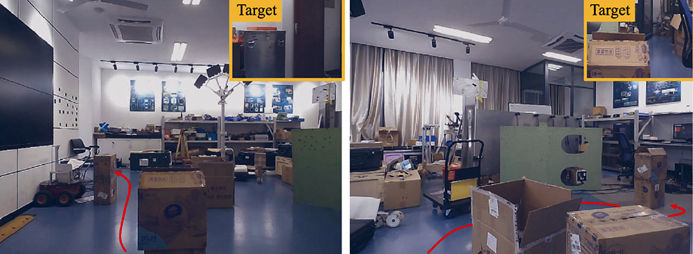
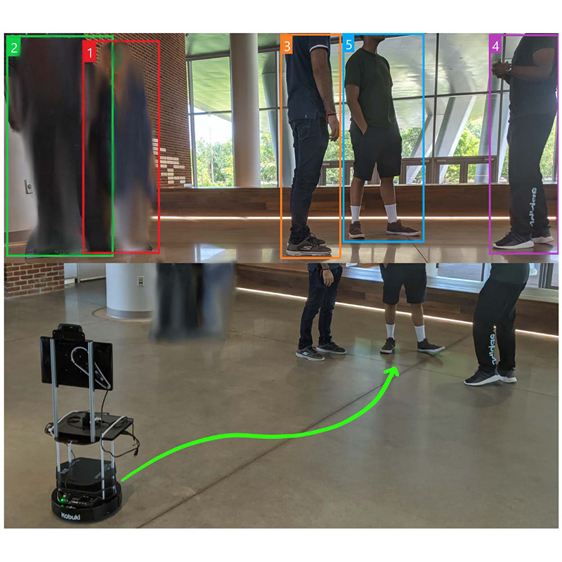
Helping robots navigate to a target, around obstacles and...
Stories / December 8, 2021
GAMMA group publishes 'COVID robot' research in PLOS One
Stories / September 9, 2020
Cornelia Fermüller is PI for 'NeuroPacNet,' a $1.75M NSF...

Stories / June 26, 2025
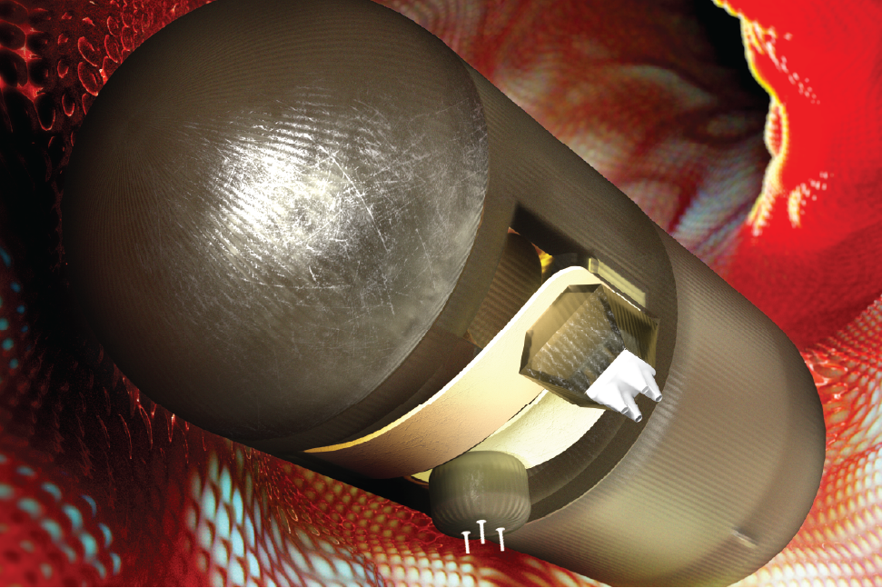
Adjustable Drug Release Marks New Milestone in Ingestible...
Stories / November 29, 2023
Alum Fumin Zhang elected to IEEE Fellow
Stories / November 29, 2023
Andrew Newman’s risk-taking work leads to Data Fusion Award
Stories / August 28, 2023
Miao Yu to develop cost-effective sensor for measuring lake...

Stories / August 16, 2023
Miao Yu receives NSF funding to develop ice-measuring sensors

Stories / July 3, 2023
ECE and ISR alumni feature prominently at American Control...

Stories / May 16, 2023
New book by Jeffrey Herrmann: Metareasoning for Robots