News Story
Srivastava part of Structured Array Hardware for Automatically Realized Applications program

ISR Director and Professor Ankur Srivastava (ECE/ISR) is part of the large “Structured Array Hardware for Automatically Realized Applications (SAHARA)” program funded by the Defense Advanced Research Projects Agency (DARPA) and led by Intel Corp.
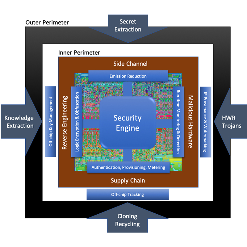
Through the SAHARA program, Intel and its partners are developing obfuscation technologies for their structured Application Specific Integrated Circuit (eASIC) chips. Srivastava is the principal investigator for a three-year, $699,830 “Red Team” subcontract that will stress test the security of these chips through rigorous verification, validation and development of new attack methodologies.
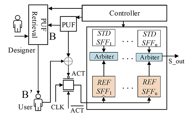
Srivastava’s team will develop strategies for attacking the integrated eASIC design flow that incorporates Logic Locking and One Time Programmable (OTP) Look-Up Table (LUT) configuration, Obfuscation, and Network on Chip (NoC) router table configuration.
About the SAHARA Program
Through automation, the SAHARA program aims to significantly improve the design flow time (from 28 weeks to 9 weeks) of converting a field programmable gate array (FPGA) chip design to Intel’s eASIC chip design. It is also incorporating and integrating four countermeasure IP security features as part of the design flow. The secured eASIC design flow will be implemented on Intel Process Technology.
About Intel eASICs
While FPGAs are field programmable, Application Specific Integrated Circuits (ASICs) are specific to each application. ASICs are designed for one purpose and cannot be changed after they are manufactured. The extra capabilities that might be used by an FPGA are not included, reducing manufacturing costs for high-volume mass production.
Intel produces “eASIC” devices, structured ASICs that are an intermediary technology between FPGAs and standard-cell ASICs. These devices provide lower unit cost and lower power compared to FPGAs and faster time to market and lower non-recurring engineering cost compared to standard-cell ASICs.
The eASICS provide lower power and unit cost by replacing SRAM configuration logic with patented single-via customization technology and disconnecting power from unused device structures. Faster time to market and turnaround time than traditional ASICs due to simplified design flow, customization of only a few mask layers, and when feasible no PCB change from base FPGA designs. The structured ASIC combines logic, memory, DSP functionality, high-speed memory interfaces, and high-speed transceivers for high-performance data plane or control plane applications.
Read more about the program in the official DARPA press release or in this story by Larry Dignan of ZDNet on the Microsoft News website.
Published December 9, 2020
Related Stories
Stories / December 1, 2020
Srivastava, Qu part of Department of Defense 'SHIP' Project...
Stories / October 28, 2020
Srivastava testing security of new delay locking technology

Stories / August 12, 2022
Srivastava named an associate editor of IEEE Transactions on...

Stories / August 11, 2022
ISR/ECE faculty organizing, moderating panel at CADforAssurance

Stories / January 26, 2022
Alum Domenic Forte featured on EE Times podcast

Stories / May 12, 2021
Alum Domenic Forte wins Yatauro Fellowship at University of...
Stories / December 1, 2020
$4.96M for Maryland researchers in DARPA AISS semiconductor...
Stories / November 30, 2020
Gang Qu elected IEEE Fellow
Stories / November 11, 2020
Work by Srivastava, Liu wins Best Paper Award at the 2020 ACM...
Stories / November 9, 2020
Gang Qu and colleagues develop method to detect recycled...